The CPUlator: https://cpulator.01xz.net/?sys=arm-de1soc.
Interrupt
ARM Interrupt in General
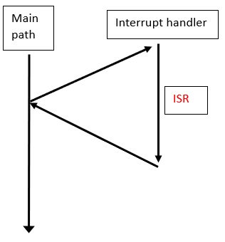
Interruption mechanism is a fundamental technique in microprocessors. It can be briefly described as a diagram in Figure 1.
ARM GIC Overview
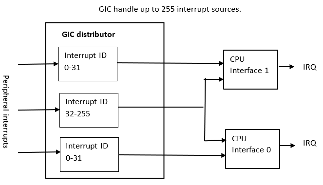
ARM Generic Interrupt Controller (GIC) is a common interrupt controller programming interface between ARM CPU and peripheral devices, and it is applicable to uniprocessor or multiprocessor systems. A device that implements GIC architecture can manage interrupts from internal or external peripheral devices. Figure 2 shows that GIC uses interrupt IDs to inform ARM CPUs. Some commonly used interrupt IDs are listed in Table 1.
| I/O Peripheral | Interrupt ID | Address |
|---|---|---|
| Interval timer 1 | 72 | 0xff202000 |
| Interval timer 2 | 74 | 0xff202020 |
| JTAG UART | 80 | 0xff201000 |
| Push buttons | 73 | 0xff200050 |
The Configuration of GIC
From Figure 2, you can realize that GIC configurations need to setup the interrupt ID and let ARM CPU know the interrupt source. GIC can handle total 255 interrupts from I/O peripherals. Some of the I/O peripherals are listed in Table 1.
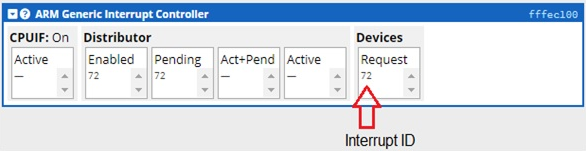
The configuration of GIC contains two portions: (1) configure Interrupt Set-Enable Registers (ICDISERn); (2) configure Interrupt Processor Targets Register (ICDIPTRn). It is not necessary to program GIC registers in this lab. In CPUlator, when you set the interrupt ID correctly, the interrupt ID will be observed from GIC panel while your code is executing. Please refer to the Figure 3 for reference.
The memory address of I/O Peripherals
I/O Peripheral addresses are pre-defined. Some of them are shown in Table 1. Those address values can also be observed from CPULator’s GUI.
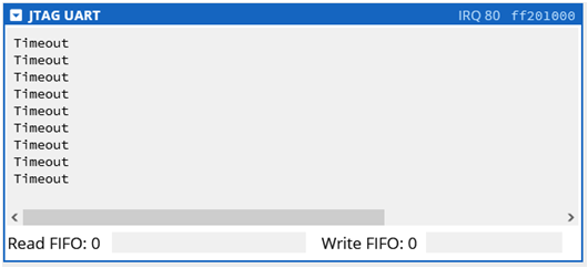
In this lab, we will use one of ARM’s interval times and UART JTAG to practice how ARM GIC works. If you complete the tasks correctly, each time when the Interval Timer times out, the panel of UART JATG displays the word “Timeout” followed by an “Enter” character (0x0A) (Figure 1). The Interval Timer times out every two seconds.
For better understanding this lab, you need to know the information of the interval timer and UART JTAG.
ARM interval timer
The timer is a peripheral that allows the user to measure real-time as a number of clock cycles. The detail information of the timers is shown in Table 1.
| Device | Timer | ||
|---|---|---|---|
| Configuration | 6 32-bit mapped registers (only lower 16 bits used) | ||
| Input/Output | Both | ||
| Address Base | Timer 1: OxFF202000 Timer 2: OxFF202020 |
||
| Address Map | Address | R/W | Description |
| base | R/W | Status Register bits: 1 - Run (1 if timer is running) 0 - Timeout (1 if timer has timed out - write 0 to this address to clear) |
|
| base+4 | R/W | Control Register bits: 3 - stop (write 1 to stop timer) 2 - start (write 1 to start timer) 1 - continue (if this bit is 1, timer will restart and continue when it times out, otherwise it will just reload the timeout period, but not start) 0 - interrupt enable for timeouts |
|
| base+8 | R/W | Period low - lower 16 bits of Timeout period | |
| base+12 | R/W | Period high - upper 16 bits of Timeout period | |
| base+16 | R/W | Counter Snapshot (lower 16 bits) | |
| base+20 | R/W | Counter Snapshot (upper 16 bits) | |
| Initialization | None (though a period must be written before running the time, or it will immediately timeout) | ||
| Interrupts | Triggered | On timeout | |
| IRQ Line | Timer 1: 0 Timer 2: 2 |
||
| Enable | Bit 0 of Control Register | ||
| Acknowledge | Read (write) interrupts acknowledged by reading (writing) to the Data register | ||
| Hardware Setup | None | ||
Note: In this lab, we use Timer 1. The full 32-bit period of the timer is given by the combination of "Periodh" and "Periodl". Both those addresses are only 16-bits, even though they take up 32-bits of the address space.
The timer counts downwards on a 100MHz clock, and runs in terms of clock cycles. For example, a period of 100000000 causes the timer to timeout in 1 second.
ARM UART JTAG
The information of peripheral UART JTAG is shown in Table 2.
Note:
The Data Register is used for both sending and receiving data —
the type of instruction executed (stw or ldw)
determines whether you send or receive. Every time you read from this
register an 8-bit data byte is ejected from the receive FIFO, and every
time you write to it you insert a byte to the send FIFO. Note that
reading the data register word obtains the "Number of Bytes available"
in bits [31:16], data valid [15], and will also read the data in bits
[7:0] and eject another byte (if any) from the queue. The "Number of
Bytes available" returns the utilization of the queue before the current
read operation.
| Device | JTAG UART | ||
|---|---|---|---|
| Input/Output | Both | ||
| Address Base | OxFF201000 | ||
| Address Map | Address | R/W | Description |
| base | R/W | Data Register bits: 31:16 - Number of characters available to read 15 - read data is valid 7:0 - the data itself |
|
| base+4 | R/W | Control Register bits: 31:16 - Spaces available for writing 10 - AC (has value of 1 if JTAG UART has been accessed by host, cleared by writing 1 to it) 9 - Write interrupt is pending 8 - Read interrupts is pending 1 - Enable write interrupts 0 - Enable read interrupts |
|
| Initialization | None | ||
| Interrupts | Triggered | On data-received or able to send (see below) | |
| IRQ Line | 8 | ||
| Enable | Set bit 1 and/or 0 in the Control Register for write and read interrupts respectively | ||
| Acknowledge | Read (write) interrupts acknowledged by reading (writing) to the Data register | ||
| Software Setup | The Monitor Program creates a terminal window automatically, that can be used to send characters to the UART and receive the output from the JTAG UART | ||
Lab Tasks
Download the assembly file l09.s. Look through this file and pay particular attention to the following items:
- vector section
CONFIG_GICconfiguration subroutineTIMER_SETTINGsubroutine.- interrupt service routine
INTER_TIMER_ISR
Then complete the following tasks:
-
Determine the initial value to be loaded to the Counter Start Value registers required to generate a time delay of 2s.
-
Complete the
TIMER_SETTINGsubroutine. In this subroutine, you should load the value determined in Task 1 to the Counter Start Value registers, initialize T0, start the timer and enable the interrupt. -
Complete the
INTER_TIMER_ISRsubroutine (Interrupt Service Routine). In this subroutine, you should write the word “Timeout” followed by an Enter character (0x0A) to UART JTAG and reset the T0 bit of the interval timer.
Zip your files together in zip file named login_l09.zip (using your Laurier login, of course) and submit that zip file to the MLS dropbox.